- 您现在的位置:买卖IC网 > Sheet目录3881 > PIC18F8585T-I/PT (Microchip Technology)IC PIC MCU FLASH 24KX16 80TQFP
PIC18F6585/8585/6680/8680
DS30491C-page 152
2004 Microchip Technology Inc.
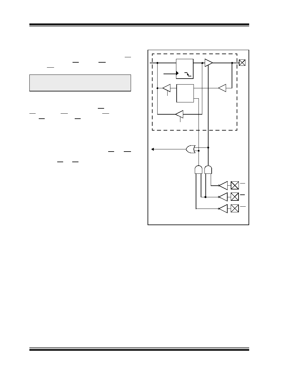
10.10 Parallel Slave Port (PSP)
PORTD also operates as an 8-bit wide Parallel Slave
Port,
or
microprocessor
port,
when
control
bit
PSPMODE (TRISE<4>) is set. It is asynchronously
readable and writable by the external world through RD
control input pin, RE0/RD/AD8 and WR control input
pin, RE1/WR/AD9.
The PSP can directly interface to an 8-bit micro-
processor data bus. The external microprocessor can
read or write the PORTD latch as an 8-bit latch. Setting
bit PSPMODE enables port pin RE0/RD/AD8 to be the
RD input, RE1/WR/AD9 to be the WR input and
RE2/CS/AD10 to be the CS (chip select) input. For this
functionality, the corresponding data direction bits of
the TRISE register (TRISE<2:0>) must be configured
as inputs (set). The A/D port configuration bits
PCFG2:PCFG0 (ADCON1<2:0>) must be set, which
will configure pins RE2:RE0 as digital I/O.
A write to the PSP occurs when both the CS and WR
lines are first detected low. A read from the PSP occurs
when both the CS and RD lines are first detected low.
The PORTE I/O pins become control inputs for
the
microprocessor
port
when
bit
PSPMODE
(PSPCON<4>) is set. In this mode, the user must make
sure that the TRISE<2:0> bits are set (pins are config-
ured as digital inputs) and the ADCON1 is configured
for digital I/O. In this mode, the input buffers are TTL.
FIGURE 10-28:
PORTD AND PORTE
BLOCK DIAGRAM
(PARALLEL SLAVE PORT)
Note:
For PIC18F8X8X devices, the Parallel
Slave
Port
is
available
only
in
Microcontroller mode.
Data Bus
WR LATD
RDx
Q
D
CK
EN
QD
EN
RD PORTD
pin
One bit of PORTD
Set Interrupt Flag
PSPIF (PIR1<7>)
Read
Chip Select
Write
RD
CS
WR
Note: I/O pin has protection diodes to VDD and VSS.
TTL
or
PORTD
RD LATD
Data Latch
TRIS Latch
发布紧急采购,3分钟左右您将得到回复。
相关PDF资料
XF2J-2424-11
CONN FPC 24POS 0.5MM SMT
PIC18LF6585T-I/PT
IC PIC MCU FLASH 24KX16 64TQFP
PIC18LF6680T-I/PT
IC PIC MCU FLASH 32KX16 64TQFP
XF2J-2224-11
CONN FPC 22POS 0.5MM SMT
PIC18F6525T-I/PT
IC PIC MCU FLASH 24KX16 64TQFP
PIC18F4439-E/ML
IC PIC MCU FLASH 6KX16 44QFN
XF2J-2024-11
CONN FPC 20POS 0.5MM SMT
PIC16LF747-I/ML
IC PIC MCU FLASH 4KX14 44QFN
相关代理商/技术参数
PIC18F85J10-I/PT
功能描述:8位微控制器 -MCU 32 KB FL 2 KB RAM RoHS:否 制造商:Silicon Labs 核心:8051 处理器系列:C8051F39x 数据总线宽度:8 bit 最大时钟频率:50 MHz 程序存储器大小:16 KB 数据 RAM 大小:1 KB 片上 ADC:Yes 工作电源电压:1.8 V to 3.6 V 工作温度范围:- 40 C to + 105 C 封装 / 箱体:QFN-20 安装风格:SMD/SMT
PIC18F85J10-I/PT
制造商:Microchip Technology Inc 功能描述:IC 8BIT MCU PIC18F 40MHZ TQFP-80 制造商:Microchip Technology Inc 功能描述:IC, 8BIT MCU, PIC18F, 40MHZ, TQFP-80
PIC18F85J10T-I/PT
功能描述:8位微控制器 -MCU 32 KB FL 2 KB RAM RoHS:否 制造商:Silicon Labs 核心:8051 处理器系列:C8051F39x 数据总线宽度:8 bit 最大时钟频率:50 MHz 程序存储器大小:16 KB 数据 RAM 大小:1 KB 片上 ADC:Yes 工作电源电压:1.8 V to 3.6 V 工作温度范围:- 40 C to + 105 C 封装 / 箱体:QFN-20 安装风格:SMD/SMT
PIC18F85J11-I/PT
功能描述:8位微控制器 -MCU 32KB Flash 2048BRAM 67I/O RoHS:否 制造商:Silicon Labs 核心:8051 处理器系列:C8051F39x 数据总线宽度:8 bit 最大时钟频率:50 MHz 程序存储器大小:16 KB 数据 RAM 大小:1 KB 片上 ADC:Yes 工作电源电压:1.8 V to 3.6 V 工作温度范围:- 40 C to + 105 C 封装 / 箱体:QFN-20 安装风格:SMD/SMT
PIC18F85J11T-I/PT
功能描述:8位微控制器 -MCU 32KB Flash 2048bytes-RAM 67I/O RoHS:否 制造商:Silicon Labs 核心:8051 处理器系列:C8051F39x 数据总线宽度:8 bit 最大时钟频率:50 MHz 程序存储器大小:16 KB 数据 RAM 大小:1 KB 片上 ADC:Yes 工作电源电压:1.8 V to 3.6 V 工作温度范围:- 40 C to + 105 C 封装 / 箱体:QFN-20 安装风格:SMD/SMT
PIC18F85J15-I/PT
功能描述:8位微控制器 -MCU 48 KB FL 4 KB RAM RoHS:否 制造商:Silicon Labs 核心:8051 处理器系列:C8051F39x 数据总线宽度:8 bit 最大时钟频率:50 MHz 程序存储器大小:16 KB 数据 RAM 大小:1 KB 片上 ADC:Yes 工作电源电压:1.8 V to 3.6 V 工作温度范围:- 40 C to + 105 C 封装 / 箱体:QFN-20 安装风格:SMD/SMT
PIC18F85J15T-I/PT
功能描述:8位微控制器 -MCU 48 KB FL 4 KB RAM RoHS:否 制造商:Silicon Labs 核心:8051 处理器系列:C8051F39x 数据总线宽度:8 bit 最大时钟频率:50 MHz 程序存储器大小:16 KB 数据 RAM 大小:1 KB 片上 ADC:Yes 工作电源电压:1.8 V to 3.6 V 工作温度范围:- 40 C to + 105 C 封装 / 箱体:QFN-20 安装风格:SMD/SMT
PIC18F85J50-I/PT
功能描述:8位微控制器 -MCU 32KB Flash 3936byte RAM RoHS:否 制造商:Silicon Labs 核心:8051 处理器系列:C8051F39x 数据总线宽度:8 bit 最大时钟频率:50 MHz 程序存储器大小:16 KB 数据 RAM 大小:1 KB 片上 ADC:Yes 工作电源电压:1.8 V to 3.6 V 工作温度范围:- 40 C to + 105 C 封装 / 箱体:QFN-20 安装风格:SMD/SMT